Directed Electrical Post-Processing of Printed Silver Ink for Improvement to Conduction and Microstructure
Authors: Vinh Nguyen, Peter H. Lewis, Brian R. Smith, Sara C. Barron, Tirunelveli S. Sriram, Gregory M. Fritz
Conference Poster Presentation: Material Research Society Fall Meeting 2017
Two of the properties limiting mass adoption of printed silver for electronics are the material's relatively low conductivity and poor electrical stability. In this work, I developed a post-processing technique that is easily implemented with commercially available silver inks and printers to increase the conductivity 2-5 times compared to traditional thermal annealing to more closely replicate the properties of extruded silver wire.
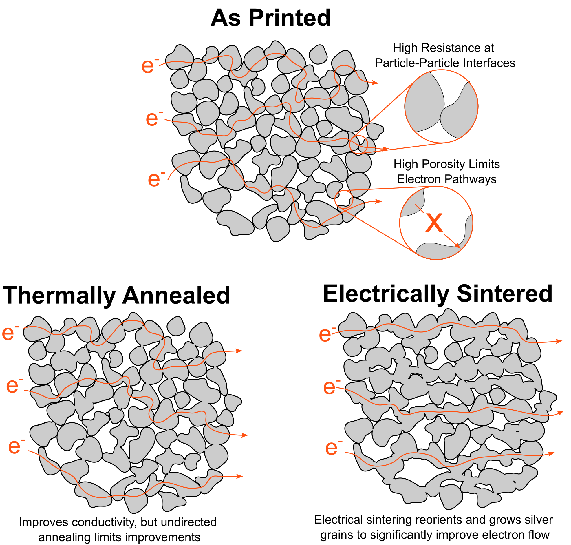
Sintering silver inks using conventional techniques results in a conductor with high porosity and particle-particle interfaces, which strongly scatter electrons. The high porosity foams suffer from small necking zones where current carrying capacity is greatly limited beyond what is expected from the nominal cross-sectional area. Furthermore, there are surface particles which are not greatly participating in the current flow since they are weakly connected to the conductive path. Post-processing is also limited by the need to protect the underlying substrate, which is often unable to tolerate temperatures above 200 ℃.
Thermal, laser, chemical, and photonic post-process annealing have resulted in significant improvements to silver inks but are undirected and result in a porous conductor. Even upon high temperature substrates, there is a limit to the improvement in conduction after anneals since excessive heating results in silver segregation as the metal reduces its surface area to volume ratio and is no longer a conductive interconnect.
At MRS Fall 2017, we presented an electrical process to improve printed silver performance without raising the temperature by more than 30 ℃. This process reorients the silver particles and grows the grain structure of the silver to significantly improve electron flow down the printed conductor. This process results in smoother traces which are more amenable to further integration into multilevel circuitry and printed electronics.
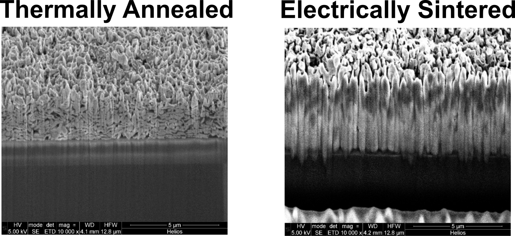
Scanning electron micrographs (SEM) of cross-sections of thermally annealed (left) and electrically sintered (right) silver traces. The thermally annealed traces have defined grain boundaries and visible voids. The electrically sintered traces have fewer voids and directional grain boundaries, which improves their electrical conductivity.